Sarcina designed this 2.5D silicon interposer package.
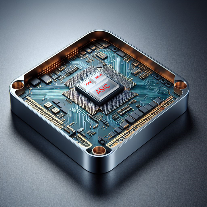
Package type: 47.5 mm x 47.5 mm HFCBGA with 2019 BGA balls
Number of die: 1 ASIC + 2 HBMs on a silicon interposer
Substrate layers: 12
Power dissipation: 320 Watts
High speed I/O: 32 lanes of 25 Gbps SerDes; 16 lanes of 16 Gbps PCIe-4
Network 2.5D Silicon Interposer Package
Sarcina optimized the SerDes Tx and Rx lane sequencing order in a package designed for a large company’s ASIC chip. Ten different divisions use this ASIC in their own networking products. Each division has their own PCB and software that require special ASIC SerDes lane sequencing.
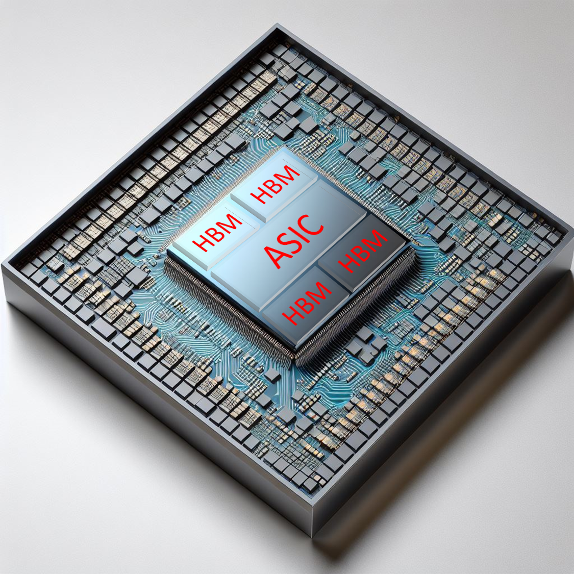
Package type: 55 mm x 55 mm HFCBGA with 2810 BGA balls
Number of die: 1 ASIC + 4 HBMs on a silicon interposer
Substrate layers: 14
Power dissipation: 400 Watts
High speed I/O: 112 lanes of 28 Gbps SerDes
Data Center High Power, Pin-Count, Performance Flip-Chip BGA Package
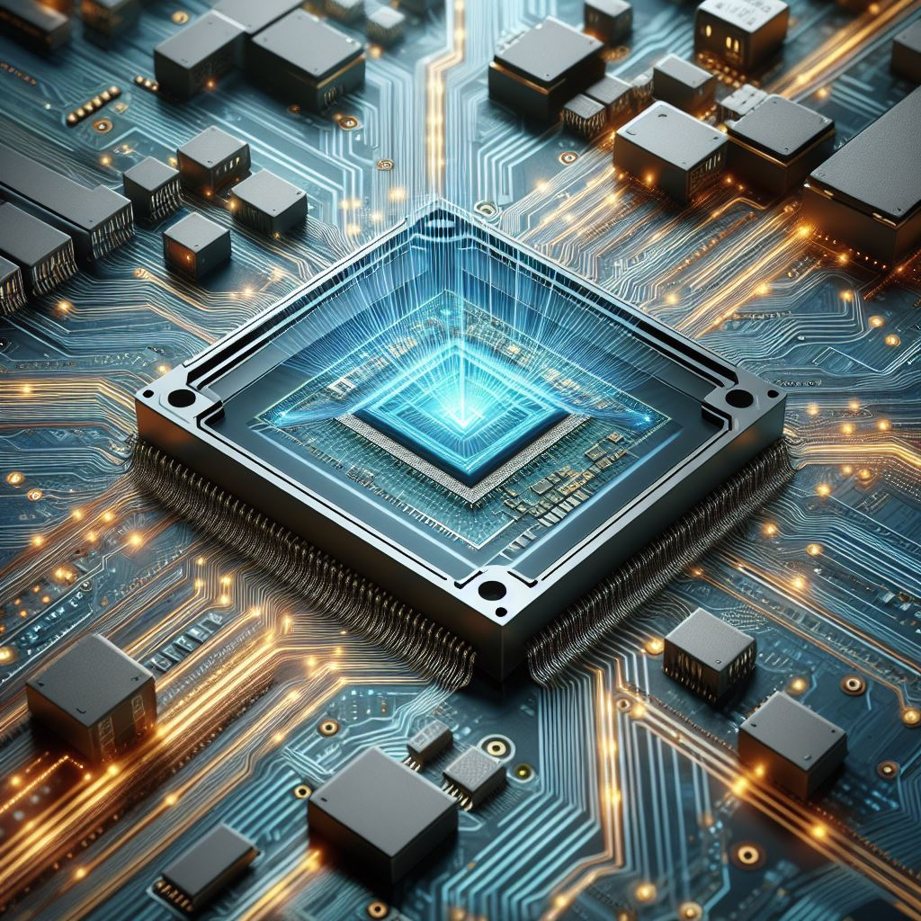
Designing LPDDR5 running at a 6400 Mb/s data rate was daunting in 2019 because the JEDEC standard was published in December, 2018. The LPDDR5 bump map was not optimized to reduce congestion in the fan out region for high I/O pin counts. The electrical simulation IBIS-AMI model was not compatible with the simulation tool. The extra eye mask margin required by the IP supplier was not realistic. On the SerDes side, 56 Gb/s data rate was considered high and implementing nearly 100 lanes of such a high speed SerDes on a single package was not easy. Sarcina’s task: design a product with many I/Os at the highest possible data rate.
Package type: 65 mm x 65 mm HFCBGA with 4092 BGA balls
Number of die: 1 ASIC
Substrate layers: 16
Power dissipation: 200 Watts
High speed I/O: 96 lanes of 56 Gbps PAM4 SerDes; 384 bits of LPDDR5 at 6400 Mbps
Today, Sarcina continues to pace the industry, taping out packages at 112 Gb/s data rates for SerDes and at 16 Gb/s data rates for GDDR6.
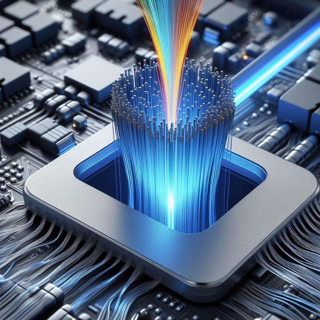
Photonic IC Package for Next-Generation Digital Communications
Sarcina has developed several generations of photonic IC packages for a tier-1 high-speed data communications customer. Today, Sarcina-designed photonic IC packages feature optical fibers directly mounted onto the photonic ICs that send/receive terabits of electrical data to/from the outside world.
Package type: 14 mm x 18 mm SiP with 336 BGA balls
Number of dice: 1 PIC, 1 ASIC and 1 Microcontroller
Substrate layers: 10 layers
High speed I/O: 4 lanes of 56 Gbps PAM4 SerDes
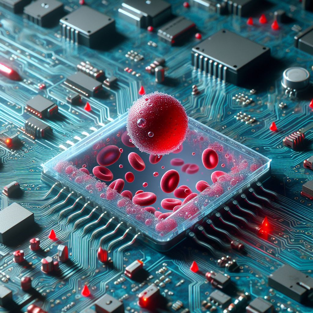
Bio-compatible Medical Package for medical Application
After two years of research, Sarcina developed several biocompatible packages that are suitable for human blood cells. Today, these packages have been used in stem-cell research, oncology, cardiology, and virology at leading US universities, research centers, and hospitals and around the globe.
Package type: 123.5 mm x 81.5 mm with 392 and 784 leads