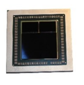
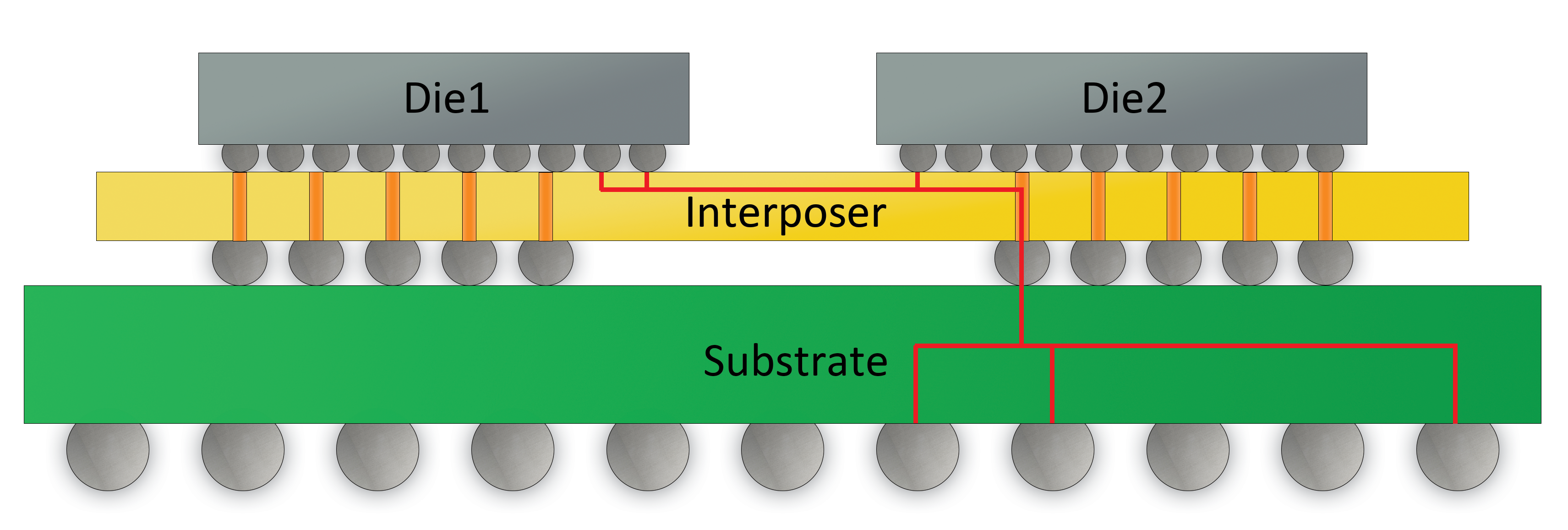
Sarcina designs 2.5D silicon interposer package for artificial intelligence, networking, and other high-performance computing applications. One of its designs in 2018 included an ASIC die and two High Bandwidth Memory (HBM) flip mounted onto a Silicon interposer. The company inserts physical test pattern into every interposer and test them on a 12″ wafer prior to assembly to increase overall yield.
3D Packaging
3D packaging integrates multiple die through traditional interconnection methods such as wire bonding and flip chip to achieve vertical die stacking. Sarcina provides both SiP (System-in-Package) and 3D WLP (Wafer Level Package) in 3D packaging with hybrid bonding pitch as small as 2 µm to reduce package size and minimize manufacturing costs.
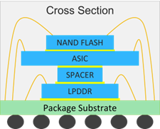
Pictured here is a 3D SiP that includes an ASIC die, a LPDDR die, and a Nand Flash die stacked inside a package. The SiP achieved a greater than 98% production yield despite the fact that there are nearly 1000 wires.
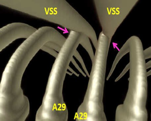
Sarcina uses 3D X-ray technology to identify and prevent wire-to-wire short.
Multi Chip Modules/Chiplet Design
Sarcina has been designing the Multi-Chip Module (MCM) packages for more than a decade. Its packages have been in production for many years.
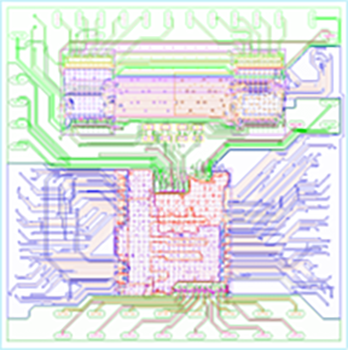
Pictured is a Sarcina package with three chiplets. It has one large ASIC die communicating to the outside world via two nearby I/O dice. Because the new I/O dice offer the next generation SerDes speed, integrating them with the ASIC extended the ASIC chip’s lifetime with little effort and at a fraction of the cost to tape out a new ASIC chip.
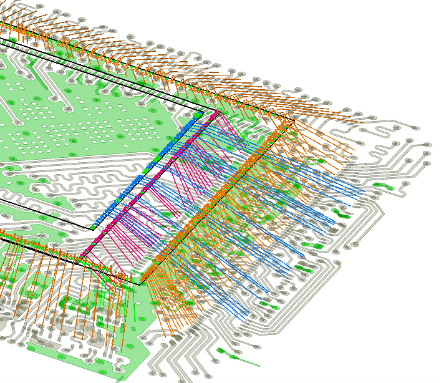
The second picture is an illustration of a package with several chiplets flip mounted on a laminate substrate, together with several passive components. A real world example is illustrated in the photonic IC package section.
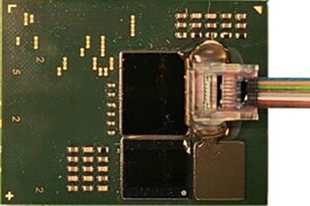
Photonic IC Packaging
Integrating lasers and photo detectors onto an ASIC silicon die to form a photonic IC (PIC) and then to integrate the PIC die with optical fibers in a package provides a more energy efficient way to increase data transmission speed and bandwidth of a digital network. It also reduces electricity costs today and lowers future hardware cost.
In this Sarcina designed package, fibers come in from right side and were coupled to the lasers on the PIC die underneath. This device allows electronic digital signals to be converted to optical signals and then transmitted to optical fibers by integrated lasers inside the PIC die.
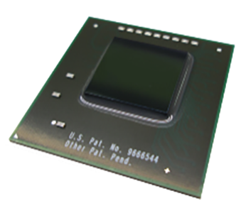
Automotive Packaging
Sarcina designs packages for automotive applications to survive stretched temperature ranges, harsh environmental conditions, and pass stringent qualification standards. These designs often require advanced packages with high I/O pin out, high communication speed, high processing performance and high power. Shown in the picture is an artist-rendered GPS chip that accurately determines a vehicle’s position and speed.
Standard Packaging
Flip-Chip BGA Package
Sarcina’s flip-chip technology features a low cost organic substrate. The company’s popular flip-chip BGA package is ideal in almost any ASIC chip with I/O frequencies exceeding 1 GHz.
Wirebond BGA Package
Sarcina wirebond package designs are found a plethora of high volume, low-cost, high-quality packages across a variety of applications. Sarcina provides this classic technology for many of today’s low speed semiconductor applications. The company also uses wirebond technology in SiP packages where several dice bonded onto a package substrate or after the bottom die is flip-chip mounted onto the substrate.
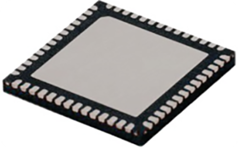
QFN Package
Sarcina uses Quad-Flat-Pack Package with No-Lead (QFN) to reduced package lead length, shrink package body size, and lower I/O parasitics. The company’s QFN designs are found in many of today’s high frequency RF packages.
Simulation
Sarcina conducts rigorous channel simulation to validate the package design before tape-out
LPDDR5/DDR5/GDDR6 Validation
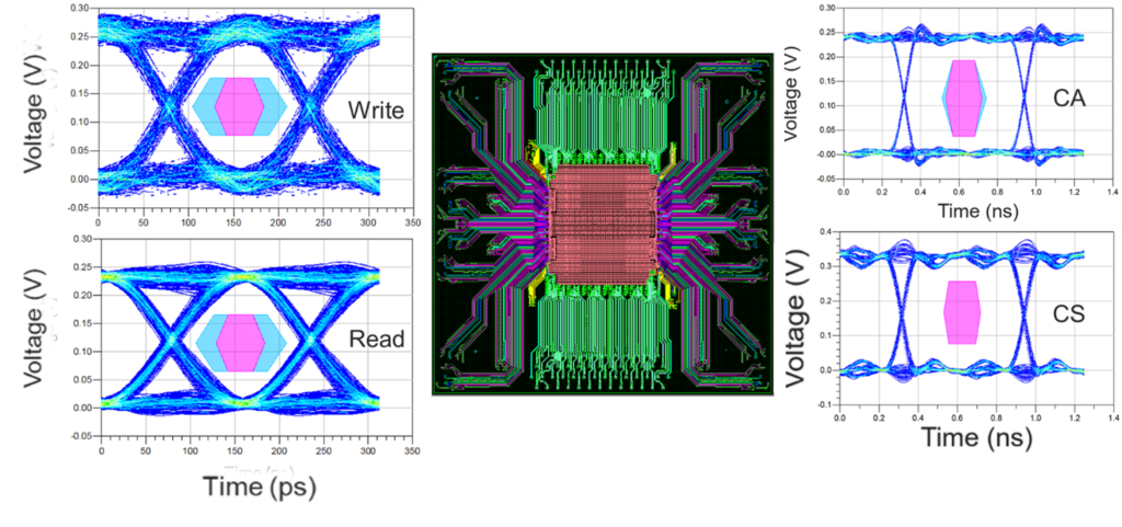
Sarcina has been developing the LPDDR5/DDR5/GDDR6 packaging technology for a tier-1 IP company for years. During this work, Sarcina developed a set of package layout guidelines and electrical design rules for bump map assignment and BGA ball map assignment, and in the areas of bump fan-out region and main routing region. In its analysis, both power integrity and signal integrity were considered in the channel simulation and the on-die decaps, the package decaps, and PCB decaps were all included.
The graphs here are our simulated eye diagrams in write and read modes for data, address and command. One routing layer was shown at the middle. The pink eye mask is the JEDEC standard. The blue eye mask shows the additional eye mask margins imposed by the IP vendor. It can be seen that our designed package met the most stringent eye mask spec. This figure demonstrates the completeness of Sarcina bi-directional channel simulation process from ASIC to memory chip and includes all components in between the two devices.
SerDes Validation
With the growing demand for higher communication speed and larger bandwidth in data transmission between devices, SerDes data transmission rate doubles every 4 years. Sarcina has successfully designed, validated and fabricated ASIC chips operating at 112 Gb/s PAM4 SerDes data rate.
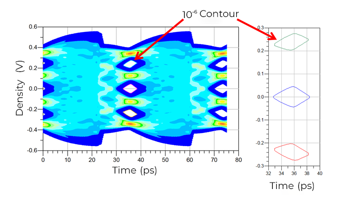
Sarcina simulation produced this channel eye diagram running at 56 Gb/s PAM4 data rate across chip, package and PCB. The plot was generated after running 1.5 million bits of data.
PCIe Validation
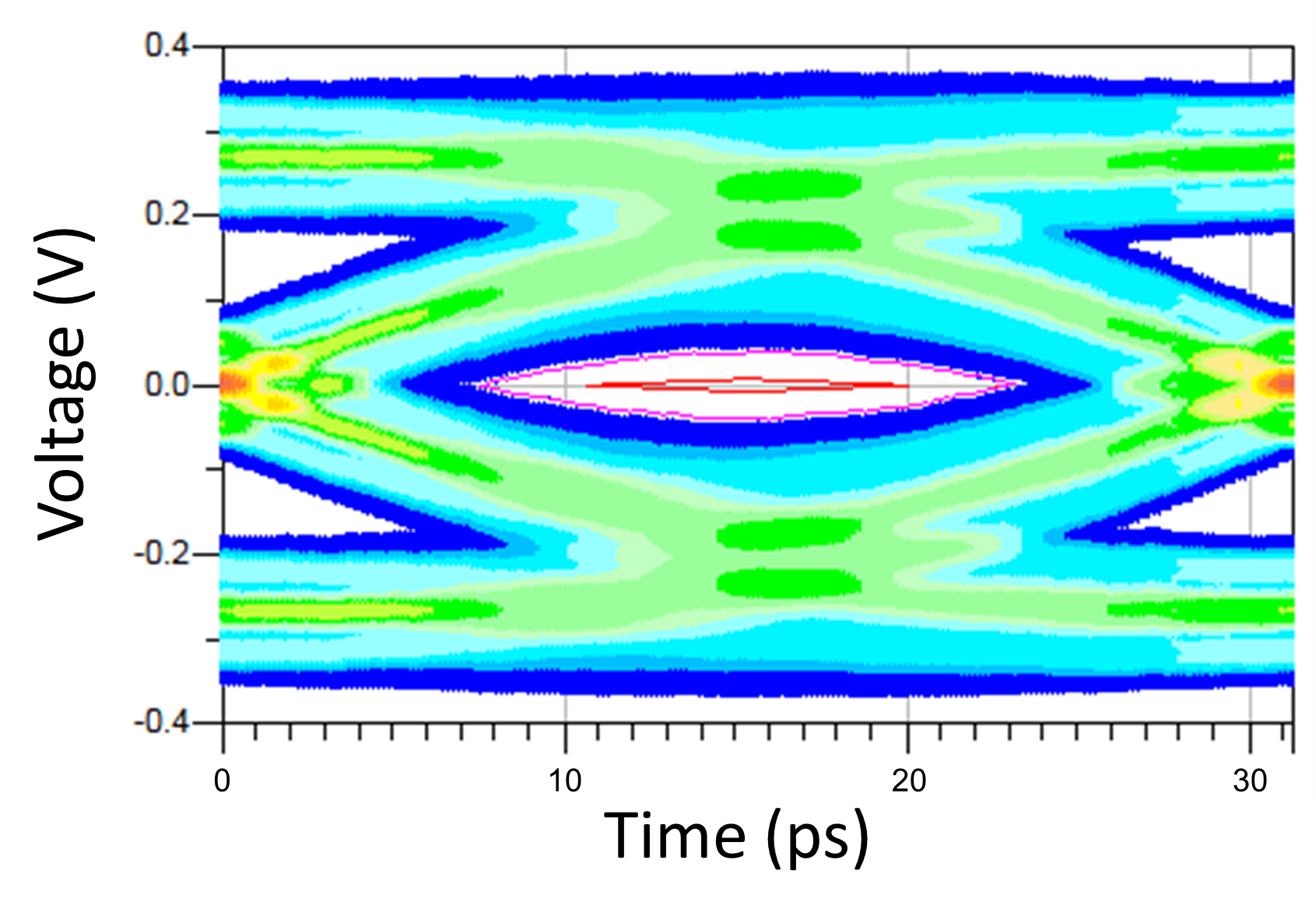
Sarcina runs a similar PCIe simulation to ensure smooth data transmission from the ASIC to other devices in a system design. Today, the company runs simulation on popular PCIe-4 and PCIe-5. Starting from PCIe-6, PAM4 could be used in data transmission. The blue eye diagram shown in the plot is for PCIe-5. It is obtained after running 10M bits of data. The pink contour is an extrapolation at 10-12 BER. The red diamond is the spec. Sarcina uses eye diagrams, similar to this one, to prove PCIe4-5 functionality.