About
Home » About
Company
When Sarcina Technology opened for business in 2011, it laid the foundation for an evolving link in the semiconductor industry value chain … the Application Specific Advanced Package (ASAP) Service.
Emerging companies in the hyper performance semiconductor market demand state of the art packaging/test capability that are tuned to very specific-product driven specs. At the same time, they want assign-it-and-forget-it dependability and high cost-to-value return. Off-the-shelf, standard semiconductor packaging clearly won’t cut it.
Sarcina built the ASAP category by providing dependable, creative, and assured solution to their advanced technology package design, test, assembly and production management services that are proven resource with a 100 percent first-time silicon success track record. Today, Sarcina Technology also provides semiconductor companies around the globe with power/signal integrity simulation, wafer probing and final test hardware design, test program development, and production services.
Sarcina works with the world’s foremost foundries to ensure high quality products and manages from the simplest to the most complex of packages. Companies forward their wafers from foundries and Sarcina does the rest. Wafers in, packaged chips out.
Management
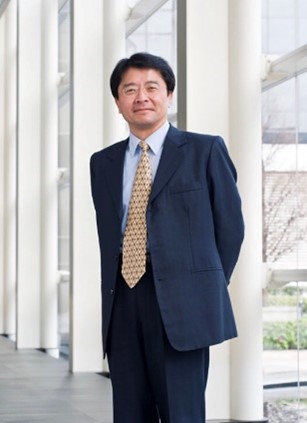
Larry Zu, Founder and CEO
Larry has grown Sarcina from designing packages for a few small companies, to doing package designs for top semiconductor companies in the world. From 2014 to 2018, Larry led the expansion of Sarcina beyond package design into final test and wafer sort hardware and software development.
Larry is semiconductor veteran who started his career at Bell Labs, before moving on to DEC, Intel, and TSMC. Along the way he developed a proven track record of delivering successful products including the Alpha, Itanium 2, Pentium 4, and XBOX 360 microprocessors. Over his career, he has taped out nearly 1,000 packages with a greater than 99% first tape-out success rate.
Larry received his B.S. in Physics from Peking University and his Ph.D. in Electrical & Computer Engineering from Rutgers University. He has many refereed IEEE publications and holds multiple U.S. patents which have been used in leading US companies’ key products.
Chuck Byers, Chief Marketing Officer
Chuck Byers is a well-known Silicon Valley Marketing executive who also holds a Lecturer appointment at the Leavey School of Business at Santa Clara University. Chuck founded the brand management team at TSMC. During his tenure, his team grew the TSMC Symposium into one of the most important events in the semiconductor industry and led a number of brand-building initiatives that helped position the company as the foundry industry leader.
Prior to TSMC, Chuck held marketing management roles at Actel Corporation and executive management and senior consulting roles at two Top-3 global marketing communications and public relations agencies.
Chuck holds a M.A. degree in Mass Communications from the University of Texas (Austin) and a B.S. in Journalism from Ohio University.
Ken Chen, Advisor
Ken serves Brillnics as its Chief Business Officer, responsible for sales and marketing. His savvy business visions, coupled with his technology leadership, has transformed Brillnics into a CMOS Image Sensor Market leader.
Prior to joining the company in 2022, Ken served as President of Global Unichip Corporation beginning in 2016. During his tenure, GUC’s valuation increased six-fold as he transformed the company into a high-performance computing IP and design service leader.
Ken transferred to GUC from TSMC in 2016 where he served in a variety of technical and business development positions, including managing the Specialty Technology portfolio that include automotive, power management, MEMS, embedded flash and display driver process technology. He also served in business development and technical marketing positioned with TSMC Japan and TSMC North America. He began his semiconductor career with Intel Corporation’s R&D Department.
Ken was awarded a Ph.D. in Materials Science at Stanford University. In 2018, he was honored as “The Outstanding President in the Hsinchu Area.”
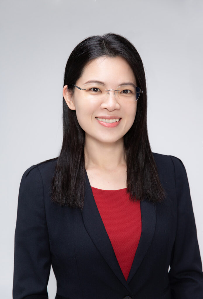
Julia Lin, Technical Director
Julia Lin manages the company’s engineering team out of Sarcina’s Taipei office. She holds overall day-to-day technical responsibility for package design, wafer sort and final test. Her supply chain management team coordinates top-tier substrate fabrication, package assembly, testing, and qualification suppliers in Asia.
Julia works with Sarcina customers to bring their product from design to prototyping and from prototyping to production. Under Julia’s supervision, all of her team’s designed and prototyped packages achieved production-proven first time success.
Before joining Sarcina, Julia worked at several leading-edge technology companies in Taiwan holding roles in package application engineering and account management.
Julia has a B.S. degree in Mathematics and a M.S. degree in Mechanical Engineering from National Taiwan University. She holds several US patents in package design.
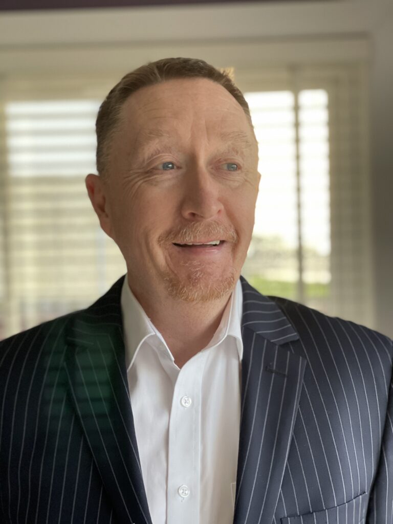
Eric Gunn, Advisor & VP Of Sales
A seasoned semiconductor executive with experience in leadership, sales, business development and marketing, Eric has worked across a number of entities within the semiconductor ecosystem including ASIC, IP, Foundry, Test/Assembly and Design Services. With over 30 years of global experience, he has held executive positions in both global Fortune 500 and start-up companies.
Eric’s track record of success includes serving as Vice President of Sales for Agile Analog, Chief Operating Officer of sureCore, Ltd. and Managing Partner of Silera, Ltd. Along the way, he also held account management roles at TSMC and guided the successful acquisition of several EDA and IP start-ups.
Eric earned his B.Sc. in Electrical and Electronic Engineer from the University of the West, Scotland.

Sarcina Design Team
The Sarcina design team is located in Taipei, Taiwan strategically close to its major foundry and OSAT partners. They are in the same time zone and speak the same language as their critical partners, responding to design, test and manufacturing issues in a timely manner. Sarcina’s world-class engineering team members have between 10 and 25 years of experience designing hundreds of packages for iconic global customers such as Broadcom, Marvell, NXP, Google, Juniper, Cadence, ZTE and H3C.
Today, millions of their packages run mission-critical computing and communication tasks around the globe.