There’s better, cost-effective path to 2.5D packaging landscape
San Francisco, CA; June 26, 2024 — Dr. Larry Zu, Founder and CEO of Sarcina Technology, the Application Specific Advanced Packaging (ASAP) Design Service and Production leader, predicted today that recent Bump Pitch Transformer (BPT) designs will speed 2.5D IC advanced packaging adoption to meet the red-hot demand for AI innovation.
In remarks made in the Keysight Theater at the 61st Design Automation Conference, he envisioned new BPT technology paving the way for new artificial intelligence computing opportunities.
“We believe that the Bump Pitch Transformer architecture will accelerate the growth rate of 2.5D semiconductor packages that are key to meeting the explosive demand for AI-driven computing capabilities,” Dr. Zu said during his address in the Keysight Theater.
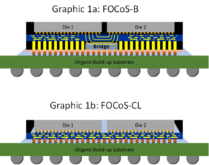
Fan-Out Chip-on-Substrate with Silicon Bridge (FoCoS-B) is the latest BPT advancement, he said, and it democratize the 2.5D era. This packaging technology is now available through companies such as ASE and SPIL, breaking a logjam of innovation created by previous proprietary BPT technologies.
FoCoS-B is a silicon bridge technology, replaces expensive silicon TSV interposers with more cost-effective re-distribution layers (RDL). This architecture is ideal for homogenous and heterogenous chiplet integration targeting high-performance computing (HPC) devices for AI, data center, microprocessor, and networking applications.
Current advanced 2.5D packaging uses a substrate to transpose an IC’s microbump pitch from 40-50 mm to the package’s 130 mm bump pitch. These substrates are very expensive, in short supply, and are complex to design resulting in lead-time and cost challenges.
The new FoCoS-B technology is effectively a Wafer Fan-out RDL technology which, due to its maturity, has inherently a lower cost and shorter lead time thus enabling system designers to optimize AI for new lower cost applications.
Sarcina is currently engaging companies with two Bump Pitch Transformer derivatives across a range of applications. Its services include BPT interposer design, O/S test pattern insertion, fabrication & BPT wafer sort, along with package substrate design, PI/SI + thermal system simulation, & substrate fabrication. A complete WIPO (wafer in, package out) engagement also covers package assembly, final test, and production services.
The company has had a number of 2.5D customer devices to successfully enter production going back several years, including a large 47.5 mm x 47.5 mm, 2,019 ball high performance flip chip ball grid array device. The total system featured an ASIC and two high-bandwidth memory chiplets HBMs on a silicon interposer and 12 substrate layers. The IC ran at 320 Watts, thanks to 32 lanes of 25 Gigabits per second (Gbps) SerDes and 16 lanes of 16 Gbps PCIe-4 interface IP.
“As amazing as this sounded several years ago, such a device is just a peek at what we’re going to see once the industry adopts the latest Bump Pitch Transformer technologies,” Dr. Zu pointed out.
About Sarcina Technology
Founded in 2011, Sarcina Technology is the Application Specific Advanced Packaging Service that provides a boutique collaborative experience for small-to-mid-sized IC companies. It boasts a proven 100% right-the-first time advanced packaging track record of wafer-to-production services that reduce overheads and speeds time-to-volume. For more information, visit sarcinatech.com

Sarcina Technology provides a choice of either silicon bridge or chip-last Bump Pitch Transformer technology options.
Media contacts


