News Room
.png)
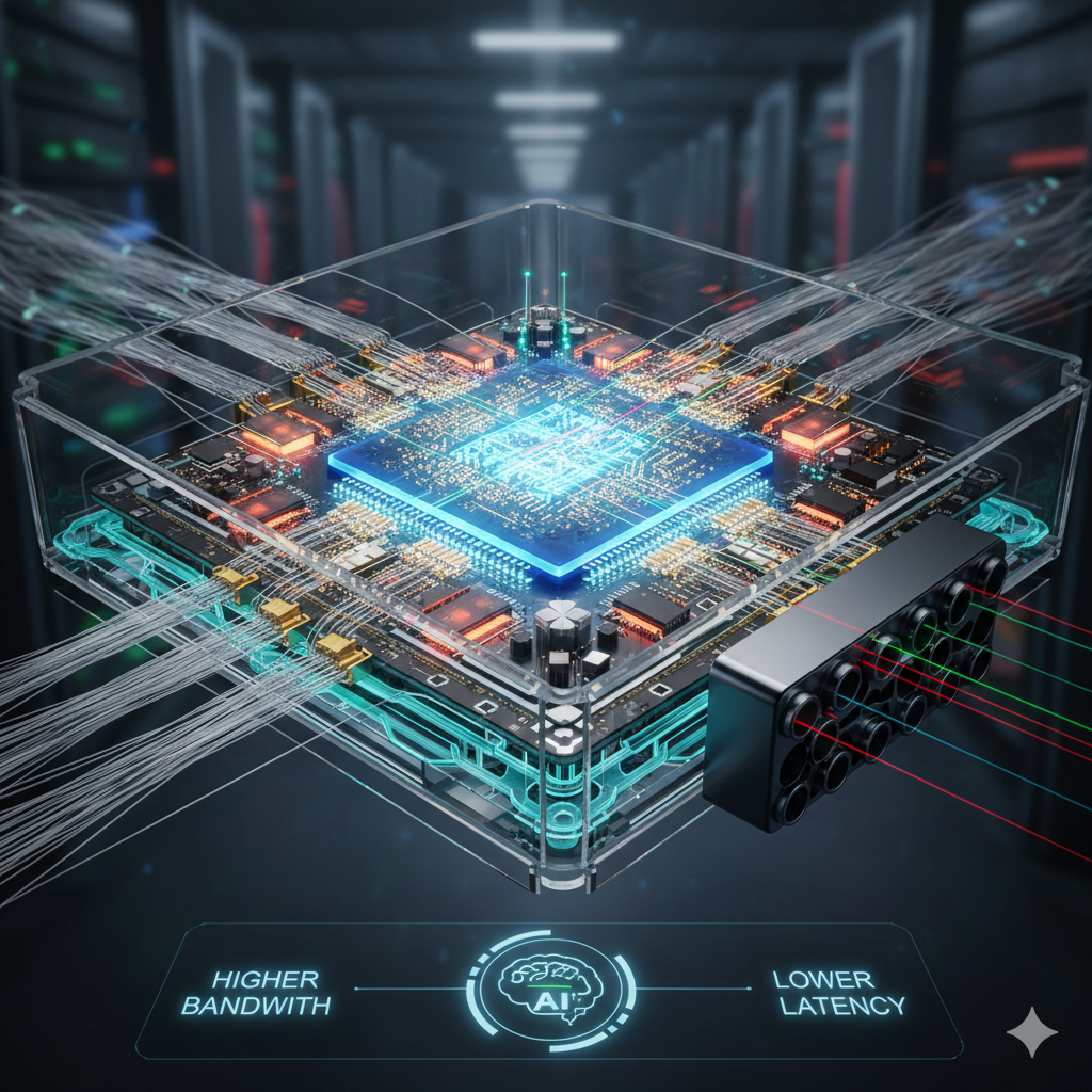
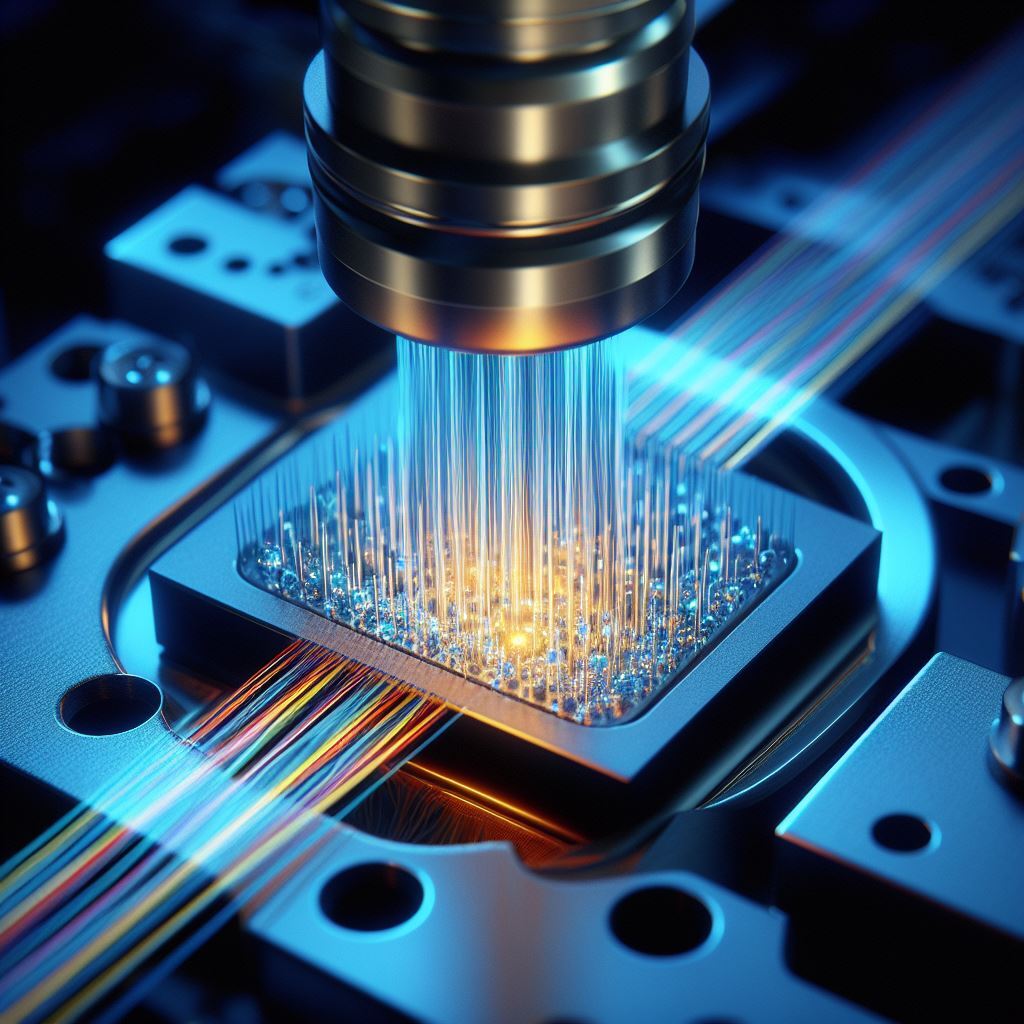
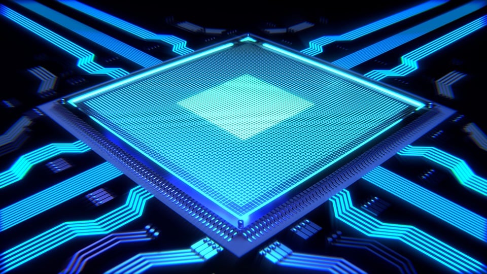
Overcoming interconnect obstacles with co-packaged optics (CPO)
Dr. Larry Zu of Sarcina Technology discusses how Co-Packaged Optics (CPO) outperforms traditional copper interconnects for AI and HPC. While CPO faces challenges in signal integrity, warpage, and alignment, Sarcina’s integrated design expertise overcomes these obstacles to enable high-speed, power-efficient data transmission.
Sarcina Technology wins 2026 Best of Show Award at Chiplet Summit
Advanced AI package design recognized for enabling scalable compute and high-bandwidth interconnect.
New Electronics: Sarcina Technology Opinion Piece
Dr Larry Zu, CEO at Sarcina Technology, outlines some of the key issues with traditional semiconductor packaging, and explains why the latest developments in photonic packaging and design are needed to meet the complex demands of AI devices.

Electronic Design Podcast: The Importance of Chip-Scale Packaging in Electronics
Dr Larry Zu, CEO at Sarcina Technology, talks with Alix Paultre at Electronic Design, about why achieving the circuit densities we need for the next generation of electronics demands advanced packaging and chip-scale interconnect solutions.
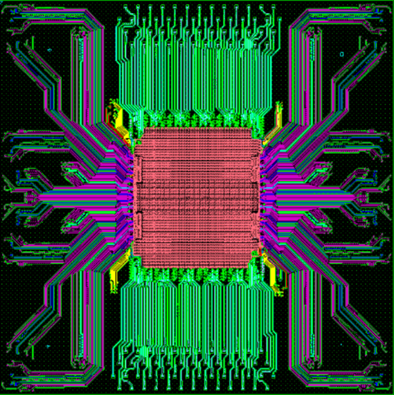
Sarcina pioneers next-generation UCIe-A/S chiplet interconnects for AI systems
With unique interposer design and advanced signal routing techniques to minimize crosstalk.
Silicon Semiconductor Interview with Sarcina CEO
Dr Larry Zu, CEO of Sarcina Technology, discusses the company’s AI platform which enables AI packaging solutions that can be tailored to meet specific customer requirements, as well as the advances in Sarcina’s photonic package design capabilities for Co-Packaged Optics (CPO).
Sarcina Technology advances photonic package design
Enabling a new era of high data rate, high bandwidth and low power interconnects
Sarcina Technology launches AI Platform
Enabling cost-effective, customizable packaging solutions for AI applications
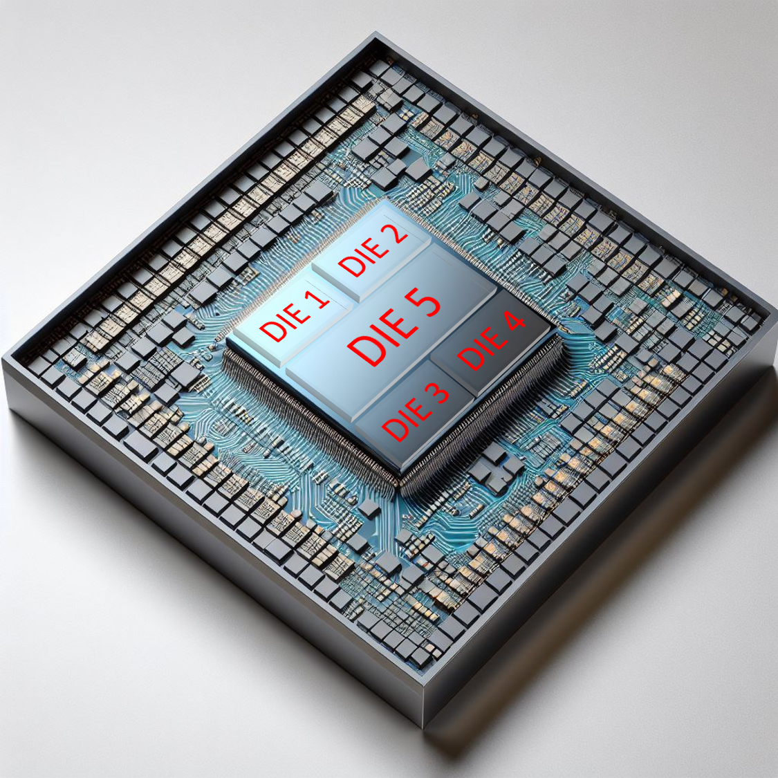
Bump Pitch Transformers Will Revolutionize Advanced Packaging
There's better, cost-effective path to 2.5D packaging landscape
Sarcina Unveils Bump Pitch Transformer Capabilities New Multi-die Technology Radically Alters 2.5D Packaging Landscape
New Multi-die Technology Radically Alters 2.5D Packaging Landscape

How Sarcina Technology Makes Advanced Semiconductor Package Design Easier
Sarcina Technology tackles the 'last mile' challenge in advanced semiconductor design with its one-stop WIPO services, delivering complex multi-die packages—from AI interposers to photonic ICs.

CEO Interview by Semi Wiki
Sarcina Technology CEO Larry Zu shares how his team delivers 100% first-time success in advanced chip packaging, tackling designs with unmatched efficiency for ASIC and system companies worldwide.

Packaging Insights Interview with CEO
Packaging Insights speaks with Larry Zu, the CEO at the semiconductor packaging business Sarcina Technology, about the development of the semiconductor packaging industry over recent years. We also discuss the current design challenges for semiconductor packaging and why the company chose Taiwan for its technology design operations.
Sarcina Technology Demonstrates Packaging Capabilities at Chiplet Summit
Showcases WIPO Services

Sarcina Technology Joins Intel Foundry Services (IFS) Accelerator Design Services Alliance
Sarcina Technology brings Application Specific Advanced Packaging Services to IFS customers.
Sarcina Technology teams up with Keysight to deliver Advanced Packages
Sarcina Technology partners with Keysight to tackle the complexity of advanced multi-die package design, using cutting-edge simulation tools to deliver first-time success on high-performance semiconductor projects.

Right-the-first-time Packages
Sarcina delivers Right-First-Time Packages using ADS for chip-package-board simulation.