Services
Wafer-in Product-out Integrated Service
Lower total packaging costs with Sarcina's exclusive WIPO service. WIPO stands for wafer-in, product-out and it eliminates the exorbitant costs of maintaining a hardware team for packaging, testing, and production. WIPO covers: wafer bumping, wafer sort, package design, test hardware design, design simulations, substrate/hardware fabrication, chips assembly, chips final test, device qualification, and production.
Key Benefits
- Faster time-to-market with integrated design, manufacturing, and testing
- Better yield, reliability, and performance through end-to-end optimization
- Lower costs by eliminating cross-vendor inefficiencies and handoff risks
- One partner for everything—simpler contracts and project management

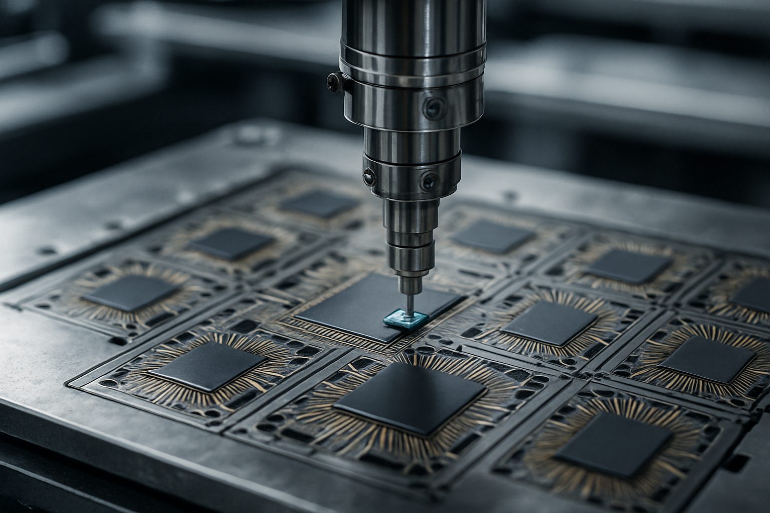
Packaging

Testing
Qualification
Production
Packaging Services
Sarcina provides a complete semiconductor packaging service portfolio.

Package Selection
Based on die information, Sarcina selects the most cost-effective package that meets your performance requirement.
Package Design
Sarcina designers develop a right-the-first time package layout that passes all electrical requirements by leveraging our patented technology and our success with more than 100 package tape outs.
Power Integrity/Signal Integrity Simulation
Sarcina's rigorous Power Integrity and Signal Integrity (PI/SI) channel simulation confirms that the package design meets all electrical requirements and spots preliminary PCB design issues.
Thermal Simulation
Sarcina's detailed package thermal model simulates the entire system's thermal performance and accurately predicts the silicon junction temperature at a given air flow speed.
Substrate Fabrication
Sarcina sends the package design to a substrate vendor and an assembly house to eliminate all manufacturing design rule violations. We then tape out the error-free package for substrate fabrication and assembly.
Package Assembly
Our local engineering team collaborates daily with assembly process engineers on the production floor during package prototype assembly to quickly resolve engineering issues and assure on-time assembly.
Testing Services
Sarcina offers one-stop testing services for all your testing needs.
Sarcina's one-stop testing service starts with a test plan. We then design, manufacture and assemble all the testing hardware, including wafer sort probe cards, final test loadboards, sockets, change kits and layout kits for Automatic Test Equipment (ATE).
Customers provide DFT test patterns that Sarcina converts to executable ATE testing files. During final test and/or wafer sort, Sarcina customizes each customer's work flow to seamlessly ramp to production.
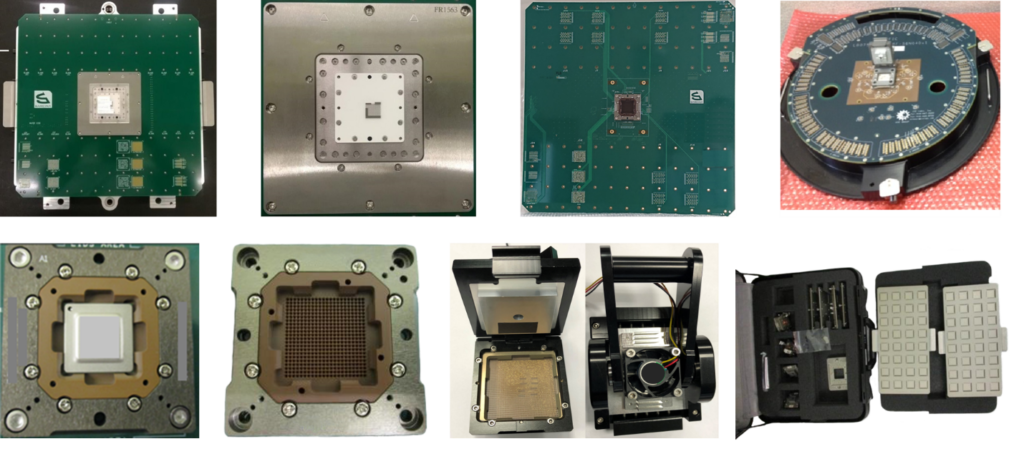
Testing Hardware
Sarcina test hardware includes (upper left two photos) a wafer sort probe card and an enlargement of the probe head. The upper right two pictures are socket-mounted final test loadboards. The square loadboard is for digital test. The round loadboard is for RF test. The lower row (left to right) shows a socket with and without a chip, a large test socket with fan, and a change kit for ATE test.
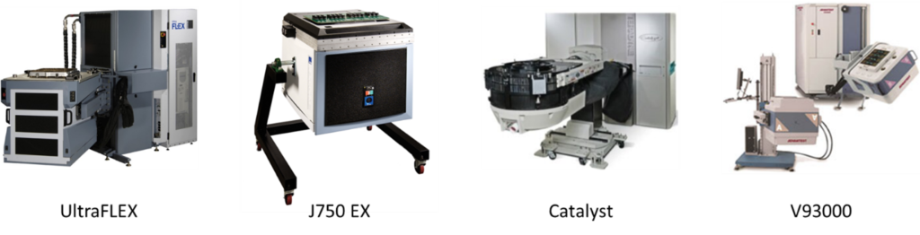
Tester Selection
Sarcina uses a variety of testers for production wafer sort and final test. These include Teradyne UltraFLEX, J750 EX, Catalyst and Advantest 93K. Sarcina selects the most cost-effective tester and proper plug-in boards for production final test.
Qualification Services
Sarcina offers two JEDEC-standard qualification services.

High Temperature Operating Life (HTOL) for IC qualification on burn-in-board (BIB)
HTOL is a reliability test used in semiconductor device qualification to assess long-term operational durability.
In this test, devices are operated at elevated temperatures (often 125 °C or higher) and under electrical bias for an extended period (typically hundreds to 1,000+ hours). The combination of heat and bias accelerates aging mechanisms such as electromigration, dielectric breakdown, and hot carrier degradation.
The purpose is to simulate years of normal use in a shorter time, identify early failures, and verify that the device meets its specified lifetime and reliability targets.

Package Qualification
Semiconductor package qualification is the process of verifying that a device's packaging — the physical enclosure, interconnects, and materials that protect the semiconductor die — can withstand the mechanical, thermal, and environmental stresses it will face during manufacturing, shipping, and field operation.
It involves subjecting packaged devices to industry-standard reliability tests (per JEDEC, AEC-Q100, or customer-specific standards) to assess robustness.
Passing package qualification confirms that the package design, materials, and assembly processes will reliably protect the die and maintain electrical and mechanical integrity over the device's intended lifetime.
Production Services
Sarcina offers comprehensive production services.
Sarcina production services reduce engineering overhead and speeds time-to-volume.
- Yield enhancement
- Wafer bumping
- Wafer sort
- Assembly
- Final test
- Failure analysis
- Return material authorization
- Logistics order
- Shipping